
- English
- Español
- Português
- русский
- Français
- 日本語
- Deutsch
- tiếng Việt
- Italiano
- Nederlands
- ภาษาไทย
- Polski
- 한국어
- Svenska
- magyar
- Malay
- বাংলা ভাষার
- Dansk
- Suomi
- हिन्दी
- Pilipino
- Türkçe
- Gaeilge
- العربية
- Indonesia
- Norsk
- تمل
- český
- ελληνικά
- український
- Javanese
- فارسی
- தமிழ்
- తెలుగు
- नेपाली
- Burmese
- български
- ລາວ
- Latine
- Қазақша
- Euskal
- Azərbaycan
- Slovenský jazyk
- Македонски
- Lietuvos
- Eesti Keel
- Română
- Slovenski
- मराठी
- Srpski језик
Sinae Cvd sic Manufacturers, Suppliers, Factory


- View as

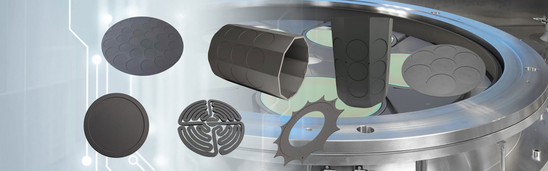
Firmus CVD Sic Rings
Semicorex solidus CVD SiC annuli magni faciunt anulum informatum principaliter adhibitum in reactione cubiculi plasmatis etching instrumenti in industria antecedens semiconductoris. Semicorex solidus CVD SiC annuli stricte subeunt electionem materialem et qualitatem temperantiae, praebens puritatem materialem singularis, repugnantiam eximiam plasma corrosionis et perficiendi operationem constantem.
Lege plusMitte Inquisitionem
Silicon Carbide Focus Rings
Pii anuli umbilici carbidi, partes anuli cruciales, specialiter ordinantur ad meliorem uniformitatem et stabilitatem lagani etching in semiconductore plasmatis etching. Celebri sunt propter excellentem observantiam in promotione uniformi plasmatis distributionis et optimizing electrici campi environment.
Lege plusMitte Inquisitionem
CVD Sic imber capitibus
Semicorex CVD SiC Shower Capita alta sunt puritas, subtilitas machinarum componentium destinata CCP et ICP etching systemata in semiconductor fabricando provecta. Semicorex eligens significat certas solutiones acquirere cum puritate materiali superiori, machinis exquisitis, et durabilitatem pro processibus plasmatis exigentibus.
Lege plusMitte Inquisitionem
Ora annulos
Semicoreex Edge annulos confidebat per ducens semiconductor facs et oems worldwide. Cum stricte qualitas imperium, provectus vestibulum processus, et applicationem, repulsi consilio, semicorex praebet solutiones extend tool vitae, optimize laganum uniformitatem, et auxilio processistis processum nodorum. *
Lege plusMitte Inquisitionem
Gas distribution laminis
Semicorex Gas distribution laminis, factum ex CVD sic est a critica component in Plasma Etching systems, disposito ut uniformis Gas dispersion et consistent Plasma perficientur per laganum. Semicorex est confidebat arbitrium in altus-perficientur tellus solutions, offering innumerabilis materia puritas, ipsum praecisione, et sulcitibus tailored ad postulatis provectus semiconductor vestibulum. *
Lege plusMitte Inquisitionem
Firmus Sic imber capitis
Solidum SiC Shower Caput crucial component in fabricando semiconductorem, specie depositionis vaporum chemicorum (CVD) processuum designato. Semicorex, dux in technologia materiae provectae, Capita Imber solida SiC praebet quae superiores gasorum praecursoris distributiones in superficies subiectas praestant. Haec praecisio vitalis est ad consequendum qualitatem et constantiam processus eventus.
Lege plusMitte Inquisitionem
Semicorex multos annos Cvd sic producens est et unus e Cvd sic fabricatoribus et supplementis professionalis in Sinis est. Postquam emisti fructus nostros provectiores et durabiles, quae sarcinam molem suppeditant, magnam quantitatem in vivis partus praestamus. Ut enim ad minim veniam, has been provided customers with customized service. Clientes nostris contenti sunt productis et praestantibus servitiis. Sincere nos expectamus ad diuturnum negotium socium fidelem decet! Grata res emendas ex officina nostra.